Polytypism and One-Dimensional Disorder in Silicon
Carbide – a Study using Synchrotron Edge Topography
A thesis submitted to the University of London for the degree of Doctor of Philosophy in the Faculty of Science
September 2002
Birkbeck College
University of London
Malet Street
London WC1E 7HX
Abstract
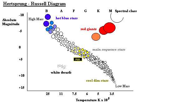
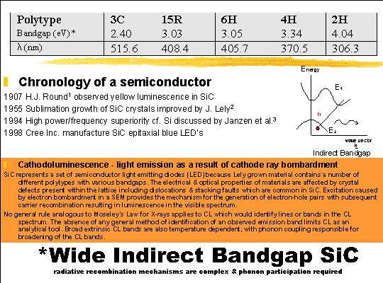
Silicon carbide (SiC)
originated before the birth of our solar system, formed in red giant carbon stars
and became trapped as interstellar grains in primitive meteorites roaming
through the Milky Way for billions of years.
Isotopic analysis of meteoritic SiC is thus offering a new and exciting
tool for exploring the structure and evolution of our galaxy. Artificial carborundum on the other hand,
manufactured as a substitute for diamonds initially, has proved more useful for
the abrasives industry, the main commercial use of SiC today. Nevertheless
interest in Moissanite gemstone production is reviving interest in this
burgeoning semiconductor material.
The current widespread interest in SiC as
a high-temperature power semiconductor can be attributed to its wide band gap
(Eg ~3 eV) electronic properties. Despite this potential, device
development has been handicapped by the presence of defects and the tendency
for SiC to form so many polytypes. The phenomenon of polytypism, first observed
in SiC ninety years ago by Baumhauer, has been studied extensively and a full
explanation for its existence still remains elusive today. The problem is
essentially that the one-dimensional ordering arrangement in SiC has produced
over 150 different layer periodicities based on the simple ABA… ABC… stacking
sequences found in close packed structures. This arises from the large number
of possible repeat sequences, the largest reported spacing in SiC being 3015 Å.
Besides these long-period ordered structures one-dimensional disorder (1DD),
when there is no finite lattice repeat, is also a prevalent feature in silicon
carbide.
A significant gap
in our understanding of polytypism exists, caused in part by the lack of
experimental data on the spatial distribution of polytype coalescence and also
by lack of knowledge of the regions between adjoining common low-period
polytypes (6H, 15R and 4H) and 1DD. Few observations detailing the relative
location of different polytypes in the same crystal have been reported.
This shortcoming has been properly addressed for the first time by constructing
morphologically accurate models of the layer-stacked SiC edges. With the
advent of synchrotron radiation source x-ray diffraction edge topography
(SRS-XRDT) and the improved resolution currently available, finer
features have been revealed at polytype boundaries. Diffraction contrast is
provided from the edges rather than the more substantial faces of the hexagonal
crystals and it is now possible to identify and confidently resolve thin
one-dimensionally disordered layers (as thin as 5 µm) and regions of
high defect density as well as long period polytypes (LPP’s).
The next nearest polytype relationships
between the common polytypes are important clues to the growth scenario of Lely
vapour grown SiC. A unique database on these adjoining polytype patterns has
prompted the author to develop a classification scheme and propose a
non-degenerate polytype-polytype configuration termed a sandwich model. These
ubiquitous features are illustrated with several examples and some general
trends and rules of polytype coalescence in SiC are presented.
Acknowledgements
The EPSRC for funding, CLRC for facilities, Prof. Paul Barnes for encouragement and friendship over many years, Dr. Graham Fisher for guidance and tuition in the early days, Dr. Graham Clark and Dr. David Laundy for help on station 7.6 of the Daresbury Laboratory SRS, Emeritus Prof. Alan MacKay for some critical inspiration and the Industrial Materials Group Birkbeck for their humour and support, in particular Dr. Jeremy Cockcroft for helpful discussion throughout my time at Birkbeck College. I am indebted to Juliet Munn, Andy Beard and Martin Vickers for their help in the SEM work.
I would also like to take this opportunity to thank the following institutions and organizing committees for the financial support and opportunity they granted me, during the course of this project, to attend the conferences and meetings listed:
Aperiodic
2000 organizing committee
Birkbeck
College Awards
The
British Crystallographic Association (BCA) in particular Prof. Chick Wilson
The
Engineering and Physical Sciences Research Council (EPSRC)
The
European Crystallographic Association
The
Institute of Physics (IoP)
Meetings:
BCA
meeting 3-5 April 2000 Edinburgh
APERIODIC
2000 conference 4-8 July 2000 Nijmegen, Netherlands
IoP
EMAG meeting 6 September 2000 London
IoP
CMMP conference 18-21 December 2000 Bristol
Royal
Society discussion meeting 21 February 2001 London
BCA/CCG
course 30 Mar-7 April 2001 Durham
BCA
meeting 7-10 April 2001 Reading
SiCEP
program 31 May-10 June 2001 Linköping/Stockholm, Sweden
ECM20
conference 25-31 August 2001 Kraków, Poland
Higher European Research Course
for Users of Large Experimental Stations (HERCULES) course 17 Feb-28 Mar 2002
Grenoble, France
Contents
Abstract
2
Acknowledgements
4
List of Figures
8
List of Tables
10
List of Abbreviations and Symbols
11
1.1
Background –
A brief History of Silicon Carbide
12
1.2
Introduction
17
1.3
A description of silicon carbide
22
1.4
On the origins of polytypism
27
1.5
Axial Next Nearest Neighbour Ising model (ANNNI)
37
1.6
Methods to study polytypes
46
1.7
Current Research
52
Chapter 2.
X-Ray
Diffraction Topography–Methods of Analysis
2.1
Introduction
54
2.2
The Early History of Topography
54
2.3
Development
of Instrumental Techniques
58
2.4
Topographic
Contrast
61
2.5
Synchrotron
Radiation Sources
65
2.6
Synchrotron Topography
69
2.7 Edge Topography
75
2.8
Photographic emulsions
78
2.9
Standard Indexed Topographs
80
2.10 Polytype Identification
83
2.11
Measuring Long Period Polytypes
88
2.12
Resolution Limit in Synchrotron Topography of SiC
90
2.13
Orthogonal Configuration
92
Chapter 3.
Edge Topography Survey Results
3.1
A
Brief History of the Project
94
3.2
In
Search of a Polytype Neighbourhood Classification Scheme
107
3.3
Polytype Coalescence Sandwich Models
112
3.4
Edge Morphology
117
3.5
Defect Density Bands
122
3.6
The
Missing Piece Method of Polytype Identification
128
3.7 One-Dimensionally
Disordered (1DD) Layers
139
3.8
Long
Period Polytypes (LPP’s)
146
3.9
Statistical
Trend of Polytypism
154
Chapter 4.
Silicon Carbide Cathodoluminescence
4.1
Objectives
158
4.2
Experimental
158
4.3 Electron
Microscopy of SiC 159
4.4
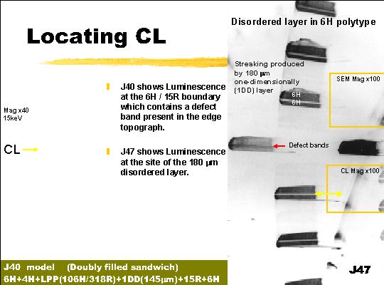
Locating
Cathodoluminescence
161
4.5
Luminescence
from 1DD layers
165
Chapter 5.
The Phenomenon of Polytypism
5.1
Summary
166
5.2
Chaotic behaviour – a model for polytypism?
168
5.3
Future
work
172
5.4
Conclusions
174
Bibliography
176
Table A1 Indexed reflections from the 31.l diffraction row for the common
polytypes 184 179
Figure A1
Graphs of INDTOP/WRIST output for 6H+4H
and 6H+15R polytypes. 185
Table A2 Polytype content
from GRF samples (pre HBL) 186
Table A3 Polytype content
from GRF samples - amended (post HBL) 187
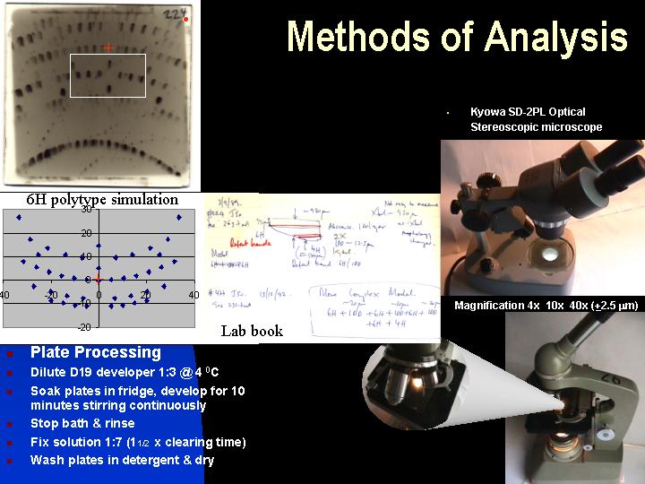
List of Figures
Chapter 1
1.1
The
Hertzprung-Russell diagram
13
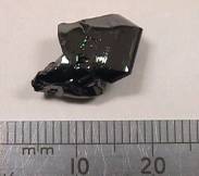
1.2
A typical silicon carbide hexagonal platelet
15
1.3
The zig-zag chain structure of hexagonal SiC
18
1.4 The relation between structure and temperature of occurrence
in SiC 20
1.5
Atomic
model of the 6H polytype of SiC
22
1.6
A
two-dimensional representation of the 1
1`20 plane in SiC 25
1.7
The spiral growth pattern of carborundum
28
1.8
Screw dislocations in silicon carbide 6H
30
1.9 Variation
of entropy with disorder in SiC 34
1.10 The
interaction scheme for the ANNNI model 39
1.11 The ground state phase diagram of the ANNNI model 41
1.12 Schematic
phase diagram of the ANNNI model at temperature kT 42
1.13 Mean field phase diagram of the ANNNI model 43
1.14
Energy band-gap diagram
50
1.15 In-situ
X-ray topography of SiC single-crystal Lely growth 53
Chapter 2
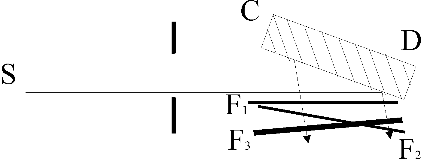
2.1
Berg-Barrett geometry
59
2.2
Lang camera
61
2.3 Schematic representation of the spectral output of the
SRS 67
2.4 Graph of the Photon flux v Energy for station 7.6 of the SRS 70
2.5 Synchrotron Radiation Source ring at the Daresbury
Laboratory 71
2.6
7.6
Topography hutch experimental layout
74
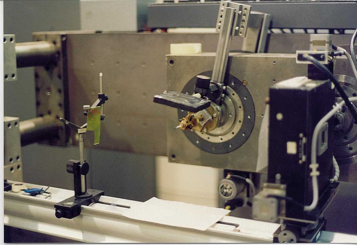
2.7 Photograph of station 7.6 hutch 77
2.8
Schematic
of experimental geometry used on station 7.6
78
2.9 Ilford L4 emulsion (full plate edge topograph of sample J50) 79
2.10
INDTOP/WRIST Simulation of 6H polytype
82
2.11
Indexed full plate topograph of 6H polytype (J112)
85
2.12
Indexed full plate topograph of 4H and 15R polytypes
(J14)
86
2.13 Multipolytypic topographs of 6H, 15R and 4H
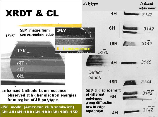
coalescence: (J52, J57) 87
2.14
Optical microscopes used in the analysis of the
photographic plates
88
2.15 Magnified long period repeat of J26 (152H/456R) 89
2.16 Geometric factors affecting resolution in a topographic
experiment 91
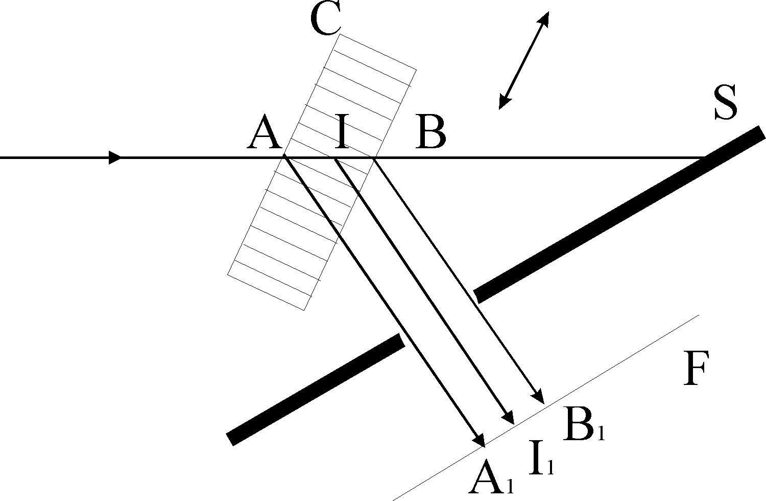
2.17 Orthogonal geometry – schematic diagram 92
2.18 Indexed full plate topograph (#389) of J26 using
orthogonal geometry 93
3.1 Photograph
of samples J1-J120 used in the edge topography survey 96
3.2
Enlargements
from a white radiation synchrotron edge topograph of J67
106
3.3
Schematic of the non-degenerate polytype sandwich
configurations in SiC
109
3.4
Photograph of a doubly filled sandwich configuration
J33
111
3.5
Simple sandwich model 6H + 1DD + 6H of crystal J6
113
3.6
Standard example of the American club sandwich model
(crystal J12)
115
3.7
A topograph of J2 showing the layer indexing of the 15R
polytype
116
3.8
Topographs and model of J26 containing an LPP assigned
152H/456R
118
3.9
Full plate edge topograph of J24 (asymmetric sandwich)
121
3.10
Topograph and American club sandwich model of sample
J52
123
3.11
A 1200μm thick SiC crystal containing the 6H polytype
(J47)
125
3.12
Topograph and model of J36 showing the presence of
defect bands
127
3.13
Illustration of the “missing piece” method of polytype
identification of J13
130
3.14 A “3-D” map of the polytype content of J13 131
3.15
Missing method applied to crystal J15
133
3.16
Unambiguous spatial polytype relationships determined
for J29
135
3.17
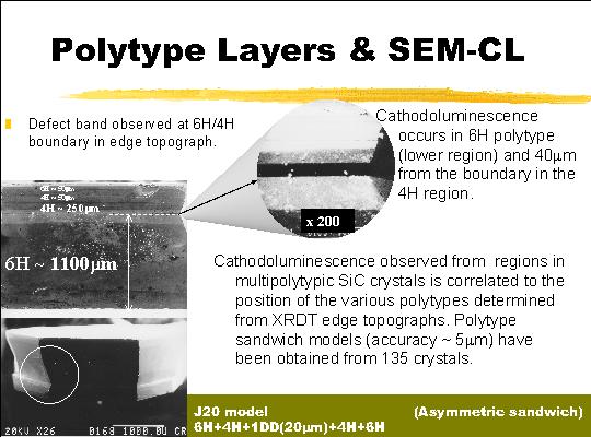
Multipolytypes in syntactic coalescence (J20)
137
3.18
An example of a highly disordered silicon carbide crystal
(J59)
140
3.19 Distribution of 1DD layer thicknesses (μm) in the
XRDT survey 142
3.20
A thin (147μm) sandwich model of J64 containing the LPP
42H
143
3.21
Enlargements from a 6H polytype (J45) containing thin
1DD layers
144
3.22a
Current status of polytype model building from SiC
synchrotron topographs
147
3.22b
Current status of polytype model building from SiC
synchrotron topographs
148
3.23
LPP 201H/603R measured in sample J105
149
3.24 LPP layer widths (μm) displayed as a function of c-repeat
spacings 152
3.25
Frequency of low period polytypes (6H, 15R, 4H)
observed in the study
153
3.26
Pie chart depicting the abundances of the various coalescence
models
155
3.27
Distribution of the crystal edge thickness data
156
Chapter 4
4.1
Photograph
of Joel JSM-35CF Scanning Electron Microscope
159
4.2
Scanning
electron micrographs of relatively thick SiC crystal edges
160
4.3
Various
micrographs of SiC crystals
(J15,
J52,
J57,
J20)
161
4.4
Complementary
combined imaging modes applied to sample J59
162
4.5
SEM
and cathodoluminescence images of J40
163
4.6
Cathodoluminescence
visible in sample J20
164
4.7
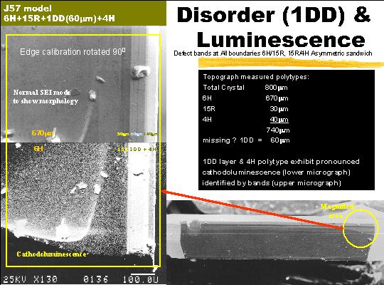
Enlarged
area SEM micrograph and CL image of J57
165
Chapter 5
5.1 Poincaré
section of a chaotic attractor (due to Ueda) 171
5.2 A
waveform plot of a solution of the Duffing oscillator 172
5.3 Plot
of LPP widths against number of layers 173
List of Tables
1.1
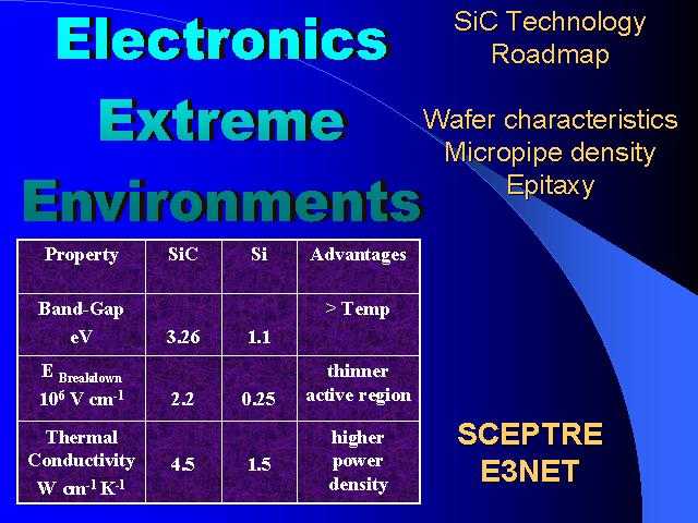
Electronics
for Extreme Environments (E3)
16
1.2 Theories
of polytypism 19
1.3 Notations
used to describe polytypes 23
1.4 Physical
properties of silicon carbide 26
1.5 Structure
series of polytypes 31
1.6 General
experimental techniques for studying polytypes 49
2.1
A
chronological summary of laboratory topography techniques
57
2.2 Calculated
X-ray photon flux on station 7.6 SRS 70
2.3
INDTOP/WRIST
output for 6H polytype
81
2.4 Systematic
absences for 6H polytype 84
2.5
Beam
size comparison (Pre/Post HBL data)
91
3.1
Detailed
assignment of all the 135 crystals used in the XRDT survey
97
3.2
Long
period polytype assignments
146
3.3 Statistical
frequency of the common 6H, 15R and 4H polytypes 153
3.4 Statistical
distribution of polytype models 155
List of abbreviations and symbols
A –
Atomic weight (g/mol ASiC = 40.10, AC = 12.01, ASi
= 28.09)
B – Magnetic flux density (Wb m-2)
B – Brilliance of synchrotron source
c – Velocity of
light in vacuum » 3x 10⁸
m s-1
C –
Polarization factor (C=1 for s polarization, C= |cos 2qB| for ppolarization)
Cd –
Contrast factor
d –
lattice plane spacing (Å)
δ
– Specimen-to-plate distance (mm)
D –
Source-to-specimen distance (m)
e – Electronic charge = 1.6
x 10-19 C
Eb – Electron beam energy (keV)
F – Structure factor (Fh)
h – Planck’s constant =
6.6 x 10⁻³⁴ Js
h,k,l
– Miller indices
I –
Integrated Intensity
I o – Incident beam intensity
l - Wavelength (nm, Å)
m –
mass (kg)
m - Linear absorption coefficient (cm-1)
x - Extinction distance
P(l) – Power in synchrotron beam
ρ – Density (g/cm3
for SiC ρ = 3.217)
re – Classical
electron radius (e2/mc2)
R –
Resolution (Rs)
Re – Depth of electron in material (μm)
s
- Standard Deviation
(S.D.)
S – Source size
t -
Thickness of sample
T –
Period of oscillation
q - Bragg angle (qB)
V –
Volume of unit cell
VD – Volume of defect
ω – angular frequency
Z –
Atomic number (Z = 20 for SiC, Zc = 6, ZSi = 14))
[ ] – denotes a Figure in
the thesis