Correlation between layer thickness and periodicity of
long polytype coalescence in silicon carbide
J.F. Kelly, P.
Barnes
Industrial
Materials Group, School of Crystallography, Birkbeck College, University of
London, Malet Street, London WC1E 7HX, U.K.
Polytypes, Silicon Carbide, Topography,
The use of synchrotron radiation source edge diffraction topography (SRS-EDT) has been developed as a technique for investigating the spatial coalescence of polytypes in silicon carbide [1]. The problem has been of long-standing concern in materials science [2], while there is renewed interest in this burgeoning wide band gap semiconductor material. Current effort underlines the importance of understanding the role of defects and disorder in polytype formation and the novel application of SRS-EDT is well suited to this task.
The use of SRS-EDT to obtain polytype profiles along with quantitative information on adjacent polytype neighbours and the regions between them has highlighted the ubiquitous nature of thin one-dimensionally disordered (1DD) layers [3]. A recent detailed study of long period polytype (LPP) coalescence [4] has enabled individual layer thickness measurements of periods up to 474H to be obtained for the first time (see Fig. 1). These results pose implications for the Lely growth of the crystals along with the comprehensive scope of the findings of this extensive survey into polytype neighbourism in silcon carbide.
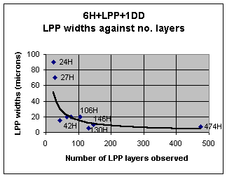
Figure1. The widths of LPP layers sandwiched between ordered and disordered regions in SiC shown against the layer stacking repeat.
References
1. Kelly J.F., Barnes P.,
Fisher G.R., Radiat. Phys. Chem. (1995), 45: 509-522.
2. Takei W.J., Francombe M.H., J. Appl. Phys. (1967), 18: 1589-1592.
3. Barnes P., Kelly J.F., Fisher G.R., Philos. Mag.
Lett. (1991), 64, no. 1, 7-13.
4. Kelly J.F.,
Barnes P., Fisher G.R., Ferroelectrics (2001), 250, 187-190.